
PCB Inspection: Methods, Defect Patterns, and Standards
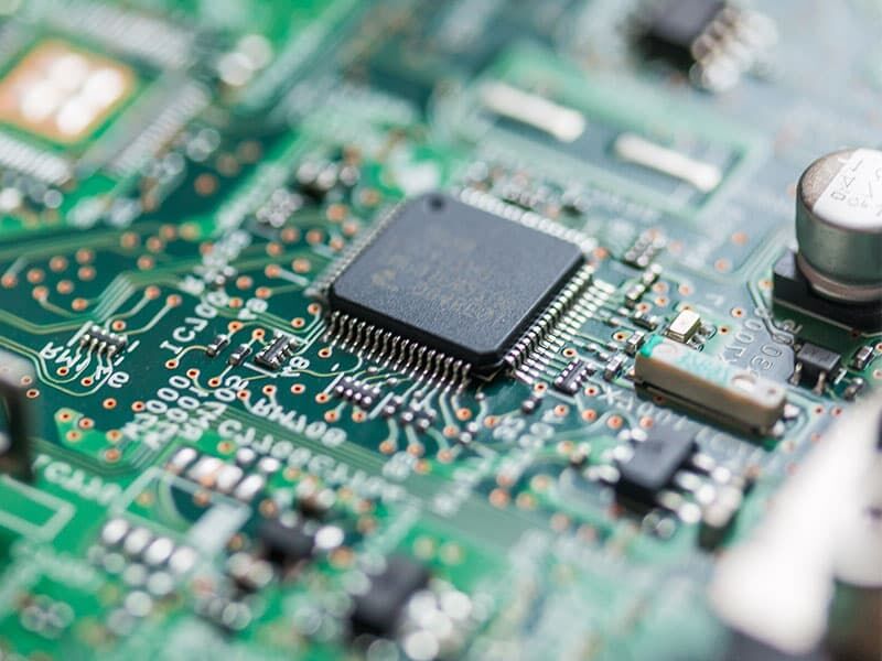
PCB inspection (printed circuit board inspection) is a collective term for optical, electrical, imaging, and analytical methods used to examine unassembled printed circuit boards and assembled electronic modules. Depending on the inspection objective, manufacturing defects, electrical deviations, internal defects, or contaminants can be detected, and potential causes of failure can be narrowed down.
Table of Contents
Contact us –
expert support is just a conversation away.
Using state-of-the-art analytical methods, we assist you with quality issues, damage claims, and development challenges – providing precise, well-founded, and solution-oriented support.

What is the purpose of PCB inspection?
Printed circuit boards (PCBs) are key components of electronic products. Defects in solder joints, conductive traces, through-holes, and layer structures , as well as residues on the surface, can impair functionality and long-term reliability. Inspections reveal such anomalies, verify electrical properties, or help pinpoint their causes.
Depending on the specific requirements, PCB inspection takes place during development, during initial sampling, during mass production, in process optimization, or as part of a damage and defect analysis. The test objective determines whether, for example, a visual or electrical production test, an X-ray inspection, or further laboratory analysis is required.
PCB Inspection
at Quality Analysis
Quality Analysis provides PCB inspection and printed circuit board analysis for PCBs and electronic assemblies using non-destructive and destructive testing and analysis methods. The focus is on imaging techniques, cleanliness analyses, and materials science investigations, which enable the localization of anomalies, the evaluation of defect causes, and the targeted assessment of manufacturing processes.
A selection of typical services in the context of printed circuit board testing:
- Analysis of solder joints, connections, and hidden structures
- Non-destructive testing using 2D X-ray inspection
- Examination of complex internal structures using 3D computed tomography
- Detection of ionic residues and filmic contaminants
- Detailed analysis using ion chromatography
- Support for defect and damage analyses
- Evaluation according to established standards and customer-specific requirements
A visual inspection captures only accessible surface features. For concealed solder joints, internal structures, contamination, or material-related weaknesses, suitable imaging, chemical-analytical, or materialographic methods are therefore combined. The choice of method depends on the defect pattern, component geometry, and desired results.
What defects can be detected during PCB inspection?
The defects that can be detected depend on the method used. While optical inspections detect visible surface and assembly defects, electrical tests check connections and functions. Imaging and analytical methods, on the other hand, reveal hidden structures or material residues.
Typical examples include:
- Defects in solder joints, e.g., insufficient solder joints, solder bridges, wetting defects, and pores or voids
- Cracks in solder joints or in the material
- Defects in BGAs, QFNs, and other hard-to-access components
- Abnormalities on traces, vias, and through-holes
- Delamination and structural anomalies in the coating structure
- Ionic contaminants and residues from manufacturing processes
- Indications of corrosion, electrochemical migration, or process-related damage
No single method covers all types of defects. For a reliable evaluation, the test objective, detection limit, and limitations of the respective method must be taken into account.
What methods are used in PCB testing?
Visual Inspection, AOI, and Microscopy
Manual visual inspection and automated optical inspection (AOI) detect accessible surface and assembly features. These include missing or misaligned components, visible solder defects, geometric deviations, cracks, and contaminants. For detailed evaluations, optical microscopy and advanced microscopic techniques are used.
X-ray Inspection and Computed Tomography
Imaging techniques examine areas that are not visually accessible. For example, 2D X-ray inspection reveals solder joints under BGAs, voids, and anomalies in through-holes in a projection image. 3D computed tomography provides a three-dimensional image of complex assemblies and reduces image overlap, but is generally more complex.
Electrical inspection and functional testing
Electrical tests check circuit traces, connections, and component characteristics. Flying-probe tests are particularly well-suited for prototypes and small production runs due to their flexible programming, while in-circuit tests with product-specific test adapters are frequently used in mass production. Functional tests then verify the behavior of the assembly under defined operating conditions.
Analysis of Ionic Contamination
Residues from cleaning, soldering, or manufacturing processes can compromise the reliability of electronic assemblies under unfavorable environmental and operating conditions. An investigation of ionic contaminants is particularly useful when contamination, corrosion, or electrochemical migration are considered as possible causes.
Ion Chromatography
Ion chromatography separates extracted ionic components and quantitatively determines individual anions and cations. This makes it possible to identify which residues are present and in what quantities they can be detected. The results are interpreted in the context of the sample area, process history, and the agreed-upon evaluation criteria.
Defect Analysis and further Material Testing
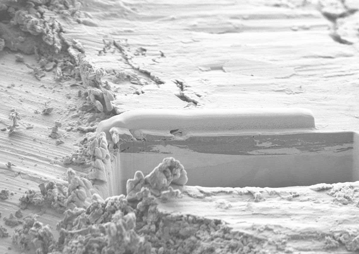
If the cause of a failure is not immediately apparent, a systematic defect or damage analysis is performed. Non-destructive testing methods are often used for localization before targeted destructive inspection is performed. This allows material weaknesses, manufacturing deviations, and stress-induced damage to be narrowed down step by step.
Which standards are relevant for printed circuit board inspection?
The evaluation may be based on IPC standards, technical specifications, drawings, and customer-specific acceptance criteria. The decisive factor is whether unassembled printed circuit boards, assembled modules, solder joints, or specific performance characteristics are being tested. The output and product class should be clearly specified in the test order.
Important standards in this context include, among others:
IPC-A-600
IPC-A-600 describes acceptance criteria for unassembled printed circuit boards. The document supports the visual evaluation of external and internal features, such as traces, holes, through-holes, surfaces, and layer structures.
IPC-A-610
IPC-A-610 specifies acceptance criteria for assembled electronic assemblies. It is used in particular to evaluate component placement, solder joints, terminals, and other visible manufacturing characteristics.
IPC-6012
IPC-6012 is a qualification and performance specification for rigid printed circuit boards. It describes requirements for design, manufacturing, and performance characteristics, thereby supplementing the visual acceptance criteria of IPC-A-600.
IPC-J-STD-001
J-STD-001 specifies requirements for materials, processes, and the design of soldered electrical and electronic assemblies. This document is relevant when evaluating the process and manufacturing requirements for solder joints.
Standards and specifications provide a framework for evaluation, but they do not replace a clearly defined test task or technical interpretation. Reliable conclusions are derived from appropriate procedures, transparent criteria, and the specific application context of the assembly.
PCB Testing in Practice
In practice, PCB inspection supports various decision-making processes: the approval of prototypes, the monitoring of mass production processes, the evaluation of customer complaints, and the investigation of the causes of failures. The inspection strategy and level of detail depend on the stage of development, production volume, risk, and agreed-upon acceptance criteria.
Typical questions include, for example:
- Are there any visible or hidden solder joints on BGAs or QFNs?
- Are there any voids, cracks, or wetting defects?
- Are there any indications of residues that could later lead to corrosion or failures?
- Do the printed circuit board or assembly meet the agreed-upon IPC criteria and the specified product class?
- What is the cause of recurring failures or variations in the manufacturing process?
A meaningful inspection therefore does not begin with the selection of a device, but with a clear set of questions. Only then can it be determined which combination of manufacturing inspection, imaging analysis, cleanliness analysis, or materials analysis is required.
FAQs on PCB Inspection
PCB inspection or testing includes both production-related inspections and more in-depth examinations. Tests typically evaluate defined characteristics or electrical functions. A PCB analysis goes beyond this and, in the case of complex failure patterns, combines multiple methods to identify causes and technical relationships.
Depending on the method used, the following types of defects, among others, can be identified:
- Defective solder joints
- Voids and sink marks
- Cracks and delaminations
- Anomalies in vias and through-holes
- Contaminants and residues
- Defects under BGAs or covered components
- Corrosion and migration phenomena
The methods used include:>/p>
- Manual and automated optical inspection (AOI)
- Microscopy
- 2D X-ray inspection
- 3D computed tomography
- Electrical testing such as flying probe or in-circuit testing (ICT)
- Analysis of ionic impurities
- Ion chromatography
- Functional testing as well as defect and damage analysis
The appropriate method depends on the test objective: Optical methods detect visible features, electrical tests check connections and functions, while X-ray, CT, and laboratory analysis examine hidden or material-related causes.
Depending on the assignment, the inspection provides measurement data, image analyses, defect classifications, or a technical inspection report. The report documents any anomalies, evaluates them based on agreed-upon criteria, and—to the extent that the available data permits—identifies possible causes and further steps for analysis.
Depending on their scope of application, IPC documents contain requirements, performance specifications, or acceptance criteria for printed circuit boards and electronic assemblies. Among others, the following are often relevant:
- IPC-A-600
- IPC-A-610
- IPC-6012
- IPC-J-STD-001
The applicable edition, product class, and evaluation criteria must be clearly specified for each individual order. IPC documents do not replace application-specific test planning.
X-ray inspection is suitable for the non-destructive examination of hidden areas, such as solder joints under BGAs, through-holes, or internal assembly structures. Since a 2D X-ray image superimposes spatial structures, 3D computed tomography may be necessary for complex geometries.
Solder joint inspection refers to the testing task, not a single method. Visible joints can be evaluated visually or under a microscope. For hidden or internal solder joints—such as those under BGAs—X-ray inspection is often used.
Ionic residues or contaminants can be analyzed, for example, using a total analysis method such as the ROSE test or selectively via ion chromatography. Ion chromatography separates and quantifies individual ionic species. The sampling method, extraction surface, and basis for evaluation must be appropriate for the test objective.
First, the issue, component, failure pattern, and available documentation are clarified. Based on this information, Quality Analysis selects appropriate non-destructive or destructive testing methods. The results are documented, technically classified, and, if necessary, verified through further testing.
Summary: PCB Inspection
PCB inspection encompasses optical, electrical, imaging, and analytical methods for unassembled PCBs and assembled modules. The appropriate method depends on whether visible manufacturing defects, electrical deviations, hidden structures, or contamination are to be examined. Quality Analysis provides support in particular with X-ray and computed tomography, microscopy, cleanliness analyses, and advanced materials science investigations. In cases of complex defect patterns, the methods are combined to produce a comprehensive analysis.